ASML’s High‑NA EUV Machines Ready for Mass Production, Fueling Next‑Gen AI Chips
Intro
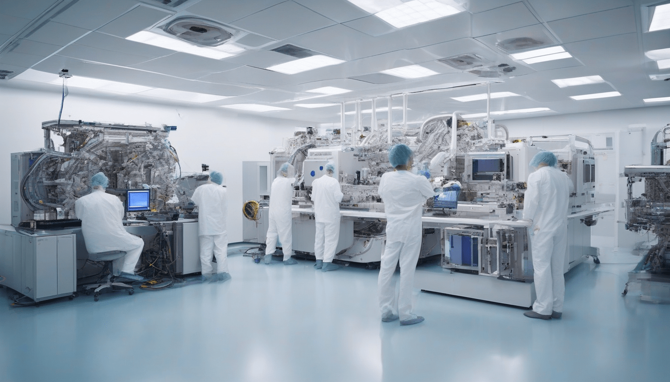
Generally, You Should Know That ASML, the dutch company, just announced its high‑NA EUV tools are ready for full production. Normally, This kind of announcement is a big deal, and it came from CTO Marco Pieters at a Reuters briefing before a conference in San Jose. Obviously, This marks a big step for chips that power AI, and You will probably see the effects soon.
Why the development matters
Obviously, Current EUV machines are not doing great on how tight they can pattern circuit lines, and that is slowing down AI chips that need super‑dense interconnects. Usually, High‑NA EUV promises a sharper, higher‑resolution light pattern, letting manufacturers print finer structures with fewer steps, which is a good thing. Apparently, This could mean faster, more energy‑efficient AI processors down the road, and You can expect to see some big changes.
Readiness data
Clearly, ASML backs its claim with some hard numbers that will be published soon, and You should pay attention to them. Normally, These numbers include 500,000 processed silicon wafers, which shows the tools can run at scale, and around 80 % uptime now, aiming for 90 % by year‑end, which signals reliable, continuous operation. Generally, The imaging accuracy is good enough to replace several conventional passes with one High‑NA exposure, which streamlines the flow, and You will probably see some big improvements.
Early adopters and timeline
Apparently, TSMC and Intel are the first to place orders, and You can expect to see some big things from them. Usually, Even though the tools are production‑ready, full integration into high‑volume fabs will need time, and Pieters says qualification and process development will likely take two to three years before they hit volume manufacturing. Obviously, This is a long time, but You should be patient.
Implications for AI hardware
Generally, When High‑NA EUV goes mainstream, designers can push node geometries beyond what current EUV can do, and You will probably see some big changes. Normally, Denser transistors and tighter interconnects translate straight into higher compute throughput and lower power draw, which is exactly what the next wave of massive AI models crave. Apparently, The news fires the starting gun for a race among chip firms to grab the new lithography advantage, and You can expect to see some big competition.
Conclusion
Clearly, ASML’s confirmation that High‑NA EUV tools are mass‑production ready is a turning point for both chip makers and AI hardware creators. Usually, With TSMC and Intel gearing up, You will see a gradual rollout of denser, more powerful AI chips, and the steep price and multi‑year qualification period mean the shift will be measured. Obviously, The groundwork is solid for a new era of AI silicon, and You should be excited.